


Pinpointing what constitutes a high-power design can be challenging. However, high-power designs generally involve currents measuring multiple amperes or voltages extending into the kilovolt range. A general guideline is to categorize designs with the potential for electrical shock or significant thermal output if not executed correctly as high-power PCB designs. In these instances, engineers must adhere to specific protocols to guarantee the safety and dependability of the product.
Poorly planned high-power PCBs present various hazards, including reduced component longevity, traces acting as fuses unintentionally, electromagnetic interference (EMI) and noise, electrical shorts due to inadequate insulation, and safety concerns.
Component Placement and Thermal Management
Careful thermal planning is the first step in optimizing high-power designs. The task involves implementing multiple measures that help spread the heat across the entire PCB and the environment to avoid thermal hotspots.
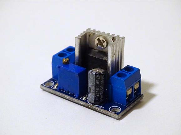
Reasonably sized heat sinks are effective in dissipating heat from components to the surrounding air.
High-power components often show more significant heat losses that require dissipation to prevent damage and reliability problems. The process starts with planning a layout that sufficiently separates the hottest components to avoid hotspots. Thermal vias help distribute the heat to the opposite layer of the PCB, and heat sinks transfer the heat to the surrounding air.
Losses and Parasitics in High-Power Designs
Traces on a PCB exhibit more significant resistive losses the longer, narrower, and thinner they are. These losses directly translate to dissipated heat; the greater the power, the more heat is generated. Further, the resistivity of materials increases with their temperature, which can further exacerbate thermal losses the longer an unoptimized circuit operates. Therefore, determining the adequate trace width and thickness is crucial for high-power PCB designs. Designers can refer to industry standards, such as IPC-2221, and online calculators to determine appropriate parameters for the power lines on a high-power PCB. Moreover, high-current PCBs also dictate the use of more or larger vias to mitigate the adverse effects of parasitic resistance.
Similarly, parasitic capacitance rises with decreasing copper weight and temperatures, so the thicker the copper traces and the better the heat dissipation, the lower the resulting unwanted capacitance — which can have tremendous impacts in high dv/dt regions such as switched nodes. Ignoring parasitic capacitance can lead to EMI, noise injection, and reduced efficiency. Designers can reduce unfavorable effects by minimizing the switched node’s copper area on the PCB, ensuring sufficient spatial separation to noise-sensitive parts, and grounding involved heat sinks, if applicable. Similarly, high-power traces should not be routed in parallel, and the overlap surface area of trace crossings should be kept minimal.
Considering parasitic inductance is crucial when designing switched current loops due to possible EMI issues and coupling problems. Keeping the high di/dt loops tight in the PCB design can help mitigate issues by preventing unwanted high-voltage spikes. Establishing low-inductance return paths by running traces above a suitable reference plane can also reduce inductance.
Increasing the copper’s surface area on the PCB, thus, leads to higher capacitance. However, doing so also decreases parasitic resistance and inductance and improves cooling. PCB designers must evaluate which method to apply to specific parts of their high-power design to mitigate certain problems without causing other unwanted side effects.
EMI Considerations in High-Power Designs
EMI problems stem from uncontrolled magnetic field coupling between inductors in a circuit. To mitigate EMI problems, designers can re-orient the inductors to provide better separation or use physical shields that block magnetic coupling between the inductors. Employing different EMI-optimized core shapes can also help in some cases.
Sensitive signal traces should be kept away from power lines by separating high-power and signal regions based on subcircuit analysis. Finally, designers should avoid placing a ground plane beneath EMI filters to prevent coupling.
Separation and Safety
Designers should refer to industry standards and guidelines for determining the minimum spacing between high-power parts of a circuit and low-power segments and user-accessible points. The exact values vary depending on various factors, such as the use case, context, voltage, insulation material, and pollution degree.
However, the main focus regarding high-power PCB safety is ensuring ample spacing between primary and secondary segments in power designs by providing wide enough physical separation gaps and keeping user-accessible points clear of hazardous voltages.
Grounding and Shielding Techniques
A fitting grounding strategy can help resolve EMI and safety issues in high-power PCB designs. Simple, low-power designs usually don’t require ground plane partitioning. However, systems that involve high currents or high voltages are an exception, and reference planes must be split between the input AC, unregulated DC, and regulated DC sections.
Furthermore, designers should consider flooding empty areas on the board with GND planes to ensure better lateral heat distribution and provide short return current paths for nearby traces and components. For that reason, designers should avoid placing slots in ground planes to prevent the disturbance of return paths and keep the parasitic inductance in check.
High-Power PCB Material Considerations
Appropriate PCB material choices matter more in high-voltage devices than in other applications, as high-voltage PCBs specifically in the kV range are subject to numerous safety and reliability concerns. Engineers can choose from different substrate materials that can withstand high voltages. Examples include BT epoxy, phenolic-cured rigid laminates, and high-voltage Teflon (HVPF).
All these materials are characterized by their ability to withstand dielectric breakdown, also known as the comparative tracking index (CTI). CTI estimates the leakage current between two conductors when the spacing is minimal. Thus, CTI defines the voltage at which an insulating material starts breaking down near its surface. Once exceeded, the material begins to carbonize and becomes more conductive, further exacerbating leakage current and breakdown over time. Industry standards like IEC 60601-1:2005 identify recommended materials for high-voltage PCBs by grouping the CTI values into categories.
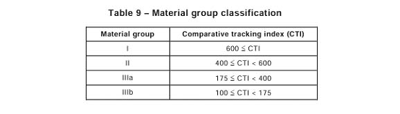
Material groups based on their CTI. Image source IEC 60601-1:2005; Section 8.9.1.7
Ultimately, the substrate material’s resin content and curing agent influence a high-power design’s resilience to common problems over time. Two common issues in high-power PCBs that use an unsuitable substrate are conductive anodic filamentation (CAF) and voids at low resin content. In CAF, high voltage encourages the electrochemical growth of conductive structures between high-potential conductors. Conversely, voids at low resin content increase the chance of degradation between the PCB stackup layers.
Higher resin content with a looser fiber weave, as a result, is generally preferred in high-voltage designs. Similarly, finer glass weaves like 1080, 2113, or 2116 are ideal. Opting for thicker boards can have multiple positive effects, as they increase the separation between conductive layers and offer more thermal mass and mechanical strength — often beneficial when using bulkier high-power components. Finally, the copper surface finish should be as smooth as possible, as rough interfaces create areas that promote static charge accumulation.
Summary
Managing thermal considerations, EMI, and safety concerns are paramount in high-power PCB designs. Effective thermal planning involves dispersing heat across the board and strategically utilizing thermal vias and heat sinks.
Optimizing trace width and thickness minimizes resistive losses and mitigates thermal issues. Parasitic capacitance and inductance must be carefully managed through proper layout and design techniques to prevent EMI and coupling problems. Grounding strategies, including partitioning and flooding with ground planes, aid in EMI mitigation and heat dissipation.
Material selection is critical for high-voltage PCBs, with substrates like BT epoxy and high-voltage Teflon chosen for their ability to withstand dielectric breakdown. Comparative tracking index (CTI) values guide material selection, ensuring safety and reliability. Resin content and curing agents influence a design’s resilience, and higher resin content and finer glass weaves are preferred to mitigate issues like conductive anodic filamentation and voids. Thicker boards offer increased separation between layers and better thermal management. Smooth copper surface finishes minimize static charge accumulation. Adhering to industry standards like IPC-2221 and IEC-60950-1 aids in material selection and design optimization for high-power and high-voltage PCBs.
